
Photonic and Plasmonic Devices
Current research interests reach from high speed modulators and photodetectors for optical communications systems to integrated laser sources and sensors for biophotonic applications. The focus is on design, fabrication and characterization of Silicon Photonic and Plasmonic devices which cannot be realized using current CMOS processes in established semiconductor foundries. To this end, we employ latest generation multiphysics simulations tools to verify our device concepts numerically. The concepts are then realized on the silicon (Si) or silicon nitride (Si3N4) material platform using state-of-the-art semiconductor fabrication processes like electron beam lithography (EBL) or reactive ion etching (RIE) in our cleanroom facilities. The viability of the devices is then investigated in our characterization laboratories equipped with most recent optical and electronic instrumentation.
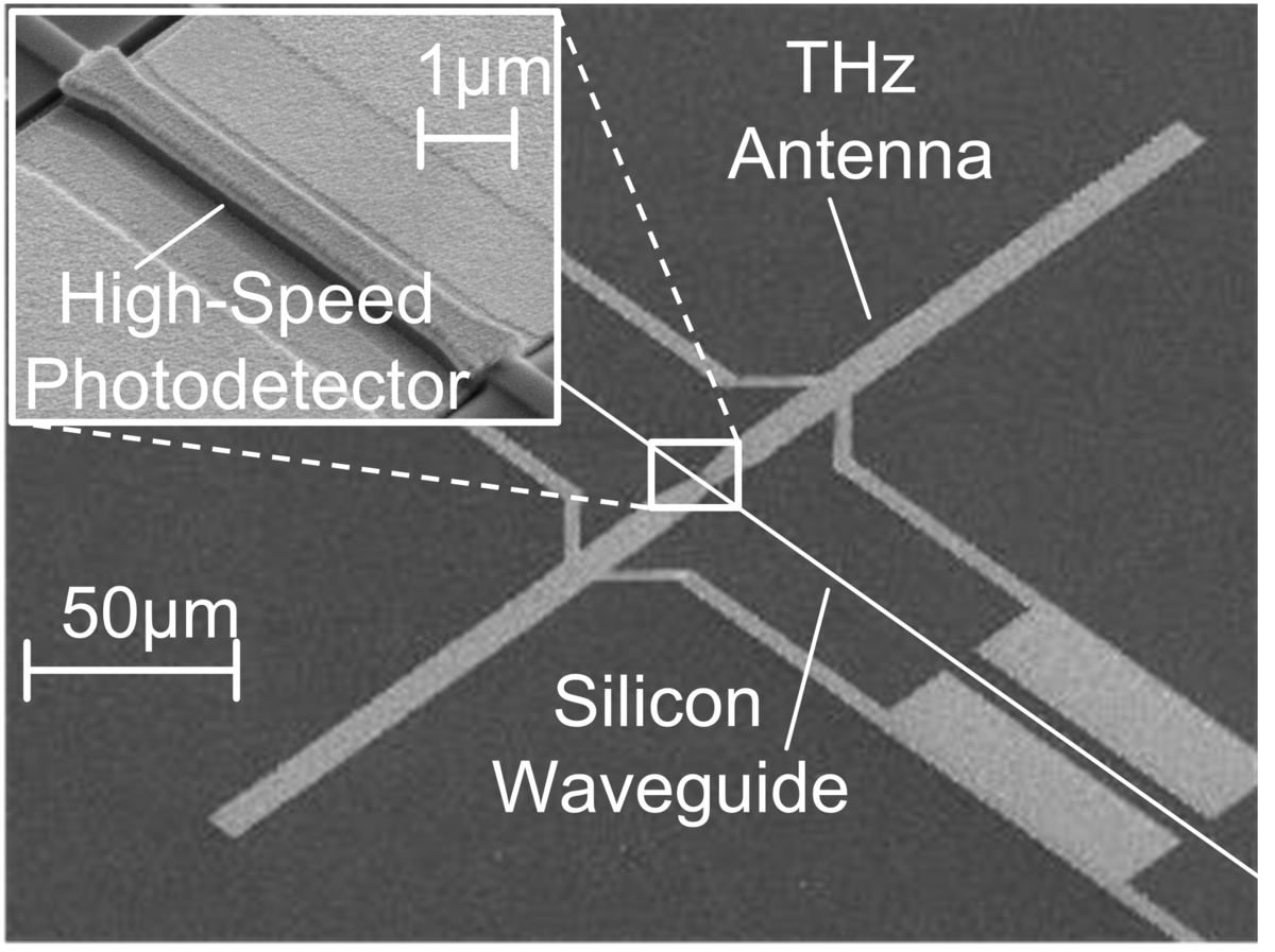
Teratronics ultimately targets at the generation, processing and detection of data at rates in the Tbit/s regime and of signals with THz bandwidths. To this end, novel nanophotonic and electronic methods are developed and their viability is tested in pioneering experiments. Teratronic devices constitute the building blocks of novel high-speed opto-electronic signal processing and wireless communication systems that will outperform currently existing communication technologies.
| Name | Title | Function |
|---|---|---|
| Hahn, Lothar | Dr. | Advanced Nanofabrication |
| Bacher, Andreas | design conversion for e-beam lithography and operator of the e-beam |