
Additive 3D Nanofabrication
Driven by substantial world-wide research investments, tremendous progress has been made in the field of photonic integration over the last few years. Both, the continuous advances of III-V material systems and the advent of silicon photonics have enabled highly scalable on-chip integration of photonic transceiver systems. However, a technology that could cope with the associated challenges regarding photonic inter-chip connectivity is still missing, and this lack presents the main obstacle towards industrial adoption of large-scale photonic-electronic integration.
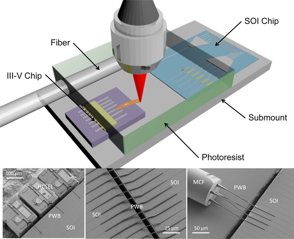
Our research on 3D photonic integration provides a novel technological approach to overcome this obstacle. The technology we developed exploits 3D in-situ structuring of negative-tone resist materials by means of two-photon polymerization (TPP). The fabrication comprises several steps: First, photonic chips are mounted on a carrier with modest precision and are partly embedded into a resist material. The spatial position of these chips is then detected by a high-precision 3D metrology system. This alignment step is in full analogy to electrical wire bonding, where high-precision machine vision systems are used to align the wire bond to metallic boards. In the next step, the geometry of the interconnect waveguide is calculated according to the exact position of the integrated chip facets and realized by nonlinear two-photon polymerization, which allows to fabricate structures with sub-wavelength precision. In a final step, the polymerized photonic wire bond waveguides are developed in a solvent bath to remove unexposed resist material. The structures can subsequently be coated with a lower-index cladding material where appropriate. This process does not only avoid high-precision passive or active positioning of photonic components with respect to each other, but also allows for the fabrication of arbitrary 3D interconnect waveguide geometries, which substantially facilitate mode field adaptation between the photonic wire bond and the planar integrated waveguides. It also allows fully automated production of interconnect waveguides with low coupling loss. In contrast to conventional optical interconnect technologies, the technology we developed neither requires high-precision alignment of optical components nor is the spatial interconnect density limited by the diameter of optical fibers.
Highlights:
Best Student Paper Competition at ECOC2019:
Optica: Terahertz optoelectronics for future wireless networks
Nature Photonics: Terahertz-to-optical conversion for future THz communication systems
ECOC 2021 Post-Deadline Paper
Nature Photonics: Terahertz Receiver for 6G Wireless Communications
| Portrait | Name | Title | Phone | |
|---|---|---|---|---|
| Bade, Klaus | Dr. | +49 721 608-24431 | klaus bade ∂does-not-exist.kit edu | |
| Bao, Yiyang | M.Sc. | +49 721 608-41935 | yiyang bao ∂does-not-exist.kit edu | |
| Maier, Pascal | Dr. | |||
| Xu, Yilin | Dr. |


| Title | Short Description | From |
|---|---|---|
| 3D Matter Made to Order (3DMM2O) | 2019-01-01 |
|
| microcomb | 2019-01-01 |
|
| PRIMA | 2017-09-01 |
|
| PIXAPP - Funding ID: 731954 | 2017-01-01 |
|
| Modeling, design and optimization of 3D waveguides (Project C4 – Wave phenomena – analysis and numerics (CRC-1173)) | 2015-07-01 |